Research Groups
Low-dimensional Quantum Materials Group
Quantum State of Matter
-
-
About
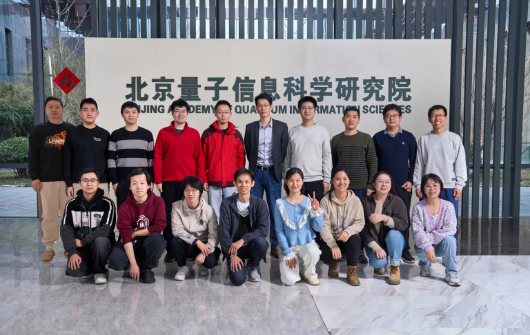
Low-Dimensional Quantum Materials Group (lab website: http://www.kaichanglab.cn/), led by Dr. Kai Chang, consists of 7 full-time members. The group is devoted to the rational design and molecular beam epitaxial growth of various functional 2D, 1D and 0D topological, superconducting, semiconducting and ferroic materials and heterostructures, as well as the ultra-low temperature scanning tunneling microscopy, optical and photoelectric studies of their physical properties and potential applications, which will consolidate the materials foundation of the downstream quantum information technologies.
Group Leader: Kai Chang
1. Scientific Research
1.1 Low-dimensional heterostructures between semiconducting, superconducting and ferroic materials
Heterostructures between low-dimensional materials are essential for modern electronic devices, including transistors, memory devices, and miniaturized sensors. These heterostructures can be formed using bottom-up methods like molecular beam epitaxy and chemical vapor deposition, or top-down methods like mechanical exfoliation-stacking and ion injection, starting from an atomically flat surface. In solid-state quantum computation, high-performance low-dimensional heterostructures such as Josephson junctions and capacitors in superconducting qubits, 2D electron gas heterostructures in semiconducting quantum dot qubits, and nanowire-superconductor heterostructures in topological qubits are required. Atomic precision is crucial for creating and characterizing these heterostructures to unleash the full potential of quantum materials.
Our laboratory focuses on growing both vertical and lateral heterostructures and superlattices between semiconductors, superconductors, ferroelectric, and ferromagnetic materials using molecular beam epitaxy (MBE), which generates atomically sharp interfaces. We observe the interfacial tuning effect through low-temperature scanning tunneling microscopy (STM), which allows us to directly see atoms and surface electronic states in real space. Our interest lies in combining atomically thin/narrow materials to generate novel quantum states of matter, such as topological superconductors, spin-textured semiconductors, and artificial multiferroics, as well as realizing functions such as tunneling memristors and ferroelectric-superconductor transistors. Our studies bridge traditional condensed matter physics and the emerging field of quantum computing.
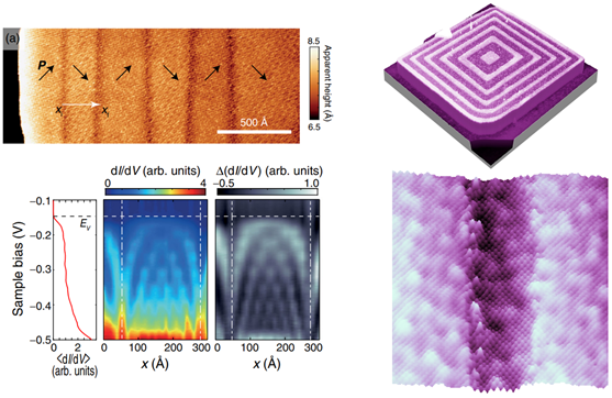
Low-dimensional semiconductors and their heterostructures/superlattices. (Left) STM topography image of a ferroelectric semiconducting SnTe monolayer with sequential 90° domains, and the corresponding dI/dV spectra across one domain revealing electronic standing waves at the valence band maximum, induced by the confinement of domain walls. (Right) Topography images of a SnTe/PbTe semiconducting superlattice. Image size: 200 nm for the upper panel and 20 nm for the lower panel.
1.2 Quantum anomalous Hall effect and its applications
The quantum anomalous Hall effect (QAHE) is a fascinating phenomenon in condensed matter physics that has attracted diverse attention and great interest in recent years. It was first predicted in the 1980s as a consequence of the quantum Hall effect, where an external magnetic field induces a quantized transverse conductance in a two-dimensional electron gas. However, unlike the quantum Hall effect, which requires a strong magnetic field to manifest, the QAHE occurs in a zero magnetic field due to intrinsic magnetization and topological properties of the material.
In a QAHE system, the electron spins align ferromagnetically, breaking time-reversal symmetry and creating a gap in the electronic energy spectrum. At the same time, a nontrivial topology of the electronic structure generates chiral edge states that run around the edges of the sample. These edge states are responsible for the quantized transverse conductance observed in experiments, while the vanishing longitudinal conductance ensures dissipation-less transport.
The unusual properties of QAHE make it an exciting area of research with potential applications in low-energy electronics, spintronics, and quantum computing. One such application is the use of QAH materials as a resistance standard operating at zero magnetic field. Additionally, QAH materials could be utilized to develop dissipationless charge/spin currents for low-power-consumption devices. Another application lies in the use of QAHE materials as quantum bits (qubits) in quantum computing, where the robustness against local perturbations like noise and disorder is crucial for reliable operation. Overall, the study of QAHE presents exciting opportunities for both fundamental research and technological application.
Despite the great triumphs achieved in the last decade, there exist several challenges associated with the study and implementation of QAHE. For example, the QAHE effect is only realized at extremely low temperatures, the mesoscopic properties of QAH materials remain largely unexplored, and finally, the long-anticipated QAHE-based Majorana zero modes, which play a pivotal role in realizing quantum computing, are still missing.
In our lab, we use state-of-the-art molecular beam epitaxy to grow QAH thin films and heterostructures, and use nanofabrication to make these films into QAH devices. We conduct cryogenic transport and spectroscopy measurements to access its electrical and magnetic properties. The ongoing project includes searching for new states of matter with high QAH temperatures, fabricating QAH devices with novel functions, exploring the diverse phases and phase transition critical phenomena in QAH materials, as well as realizing QAH-based Majorana physics.
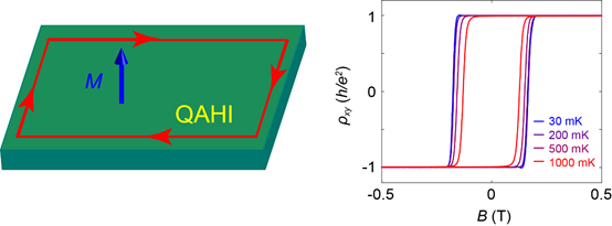
Left: schematic illustration of a QAHI, the chiral states are running on the edge. Right: field dependence of Hall resistance of a QAHI. The Hall resistance is exactly one resistance quanta h/e2, wherein h is the Planck constant and e is the elementary charge.
1.3 Low-dimensional superconductivity
Superconductivity is a fascinating macroscopic quantum phenomenon where certain materials exhibit zero electrical resistance and perfect diamagnetism below critical temperatures. A two-dimensional (2D) superconductor is a superconducting system confined to a thin, 2D plane. 2D superconductivity is of particular interest due to its quantum confinement, directional anisotropy, high critical temperature, and potential for novel electronic devices. Our focus is on preparing high-quality crystalline 2D superconductors, including interface-enhanced superconductors, topological superconductors, and monolayer superconductors. We then manipulate their properties to gain further insight into their behavior and explore ways to apply them in next-generation electronics and quantum computing.
1.3.1 Interface-enhanced superconductivity refers to the phenomenon where the superconducting properties of a material are improved when it is brought into contact with another material at the interface. The interface between the materials can modify the electronic properties of the superconductor, leading to an increase in the critical temperature. This enhancement of superconductivity has potential applications in developing more efficient energy transmission and storage systems. Monolayer FeSe on SrTiO3 exhibits a superconducting transition temperature of >40 K, which is significantly higher than the bulk FeSe. It has a unique electronic structure with a highly two-dimensional nature, which makes it an interesting system for studying the effects of dimensionality on superconductivity. The interface between FeSe and SrTiO3 can induce significant changes in the electronic properties of FeSe, including the enhancement of superconductivity. By studying this system, researchers can gain insights into the mechanisms underlying high-temperature superconductivity and explore new ways to enhance the superconductivity of iron-based materials. Additionally, monolayer FeSe on SrTiO3 as well as other related systems (e.g. FeTe1-xSex and FeTe films) offers a platform for studying the interplay between superconductivity and other phenomena, such as magnetism, nematicity and topological surface state.

(a) Topography of monolayer FeSe on SrTiO3 by STM. (b) Tunneling spectrum showing the superconducting gap. (c) Topography of FeTe1-xSex on SrTiO3
1.3.2 FeTe1-xSex is a material that has been shown to exhibit topological superconductivity. This material is a type of iron-based superconductor that can be tuned to exhibit topological properties. When the amount of Te is increased to a certain level, the material undergoes a transition from a conventional superconductor to a topological superconductor. This transition is characterized by the appearance of zero-energy Majorana bound states (MBS) at the vortex cores, which are protected by the topological properties of the material. MBS have unique properties that make them attractive for quantum computing, such as their non-Abelian statistics and their ability to encode quantum information in a topologically protected way. These properties make it possible to perform quantum operations on qubits without destroying their coherence, which is a major challenge in building practical quantum computers. Therefore, studying topological superconductivity and find establish the method to manipulate the MBS in FeTe1-xSex is a significant for the realization of topological quantum computing.
1.3.3 Disorder-enhanced superconductivity is rare and has been observed only in some alloys or granular states. Owing to the entanglement of various effects, the mechanism of enhancement is still under debate. We report a well-controlled disorder effect in the recently discovered monolayer NbSe2 superconductor. The superconducting transition temperatures of NbSe2 monolayers are substantially increased by disorder. Realistic theoretical modelling shows that the unusual enhancement possibly arises from the multifractality of electron wavefunctions. We provide experimental evidence of the multifractal superconducting state.
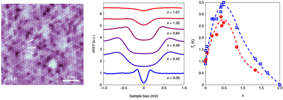
An atomic-resolved image of the NbSe2?xSx (x = 0.31) monolayer. The superconducting transition temperature as a function of x. The open squares are the gap closing temperature while the red dots are the temperatures for the disappearance of the coherence peaks.
1.3.4 Bardeen-Cooper-Schrieffer (BCS) superconductivity and Bose-Einstein condensation (BEC) are two asymptotic limits of a fermionic superfluid. We report direct spectroscopic evidence of BCS-BEC crossover in real space in a FeSe monolayer thin film by using spatially resolved scanning tunneling spectra. The crossover is driven by the shift of band structure relative to the Fermi level.
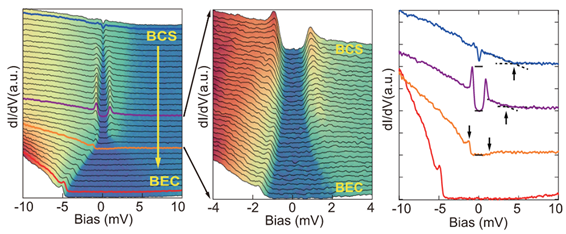
The dI/dV spectra cross the BCS-BEC region. Spectra acquired at the locations marked by colored lines. The arrows indicate the top of hole band.
1.3.5 As a two-dimensional superconductor, PdTe2 is a promising material candidate for exploring the novel phenomena of superconductivity in the two-dimensional limit. We observed a transition from the narrow-gap semiconducting phase in the monolayer to the metallic phase in the multilayer films. Importantly, all the multilayer films exhibited robust superconductivity, exhibiting high in-plane critical magnetic field, which is explained as type-II Ising superconductivity.
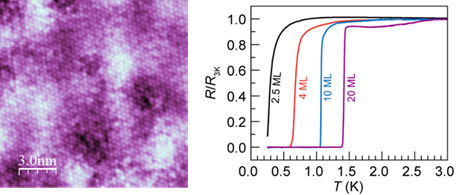
Topographic images taken on 2-ML films. Temperature dependence of the resistance of PdTe2 films with various thickness.
1.4 Optical and optoelectronic studies of low-dimensional materials
As a branch of modern optics, nonlinear optics has developed into a key technology, which proved to have many advantages in characterizing the crystal, electronic, and spins structures of low-dimensional materials, which are characterized by their ultrathin nature, high surface area, and exceptional mechanical, electronic, and spin properties. It is convenient to combine nonlinear optics and microscope techniques to image 2D materials. The focused laser spots ranging from microns to hundreds of nanometers are very suitable for most 2D materials and are highly sensitive to its weak signals.
Among the optical techniques, second harmonic generation (SHG) is one of the simplest nonlinear optical process where two photons of the same frequency combine to generate a new photon with twice the frequency. SHG can occur when a material with a non-centrosymmetric crystal structure is excited by a laser beam. In the context of 2D materials, SHG arises from the asymmetric distribution of electron charge and spin density, which leads to a non-zero second-order susceptibility tensor. Thus, it is very promising to engage SHG technique to research the structural-changing related physical process, as well as to research potential applications in areas such as ultrafast photonics, nonlinear optics, and quantum computing.
Photoluminescence is a phenomenon that occurs when a material absorbs light energy and then re-emits the energy in the form of light. In 2D materials, the electronic structure is strongly influenced by quantum confinement effects, resulting in unique optical properties. The photoluminescence emission spectrum provides valuable information about the electronic band structure and excitonic properties of 2D materials. The intensity and peak position of the photoluminescence emission can be used to extract important parameters such as the bandgap, exciton binding energy, and doping concentration.
Raman spectroscopy is a non-destructive and non-invasive technique that is widely used to study the structural, electronic, and vibrational properties of materials. In 2D materials, the Raman spectrum is highly sensitive to the number of layers, doping, strain, defects, and other physical and chemical properties. The ratio of the intensities of these peaks can provide information about the number of layers, while the position and width of the 2D peak can be used to determine the degree of disorder and the electronic band structure.
After nearly 4 years of development, the optical Lab of our team is operating normally. We have shock-isolation optical platforms, wavelength tunable femtosecond laser amplifier, OptiCool multi-functional sample cavity, grating spectrometer, etc. Based on this Lab, we have successfully built many nonlinear optical measurement systems, including far-field and microscopic SHG systems, horizontal and vertical microscopic PL systems, and a far-field SHG system based on OptiCool, and many scientific research results have been produced.

(a) Principle diagram of SHG and (b)(c) Polarized anisotropy SHG images acquired from different BiFeO3/SrTiO3 heterostructures. As the thicknesses of BiFeO3 films increase, its crystal structure vary from Tetragonal to Monoclinic, which can be verified by the features of SHG images.
2. Lab facilities
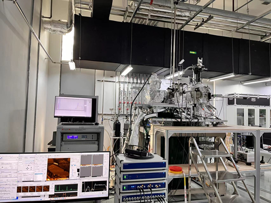
Ultra-low temperature STM-MBE system (Unisoku USM1300, 0.4 K, 9-2-2 T)
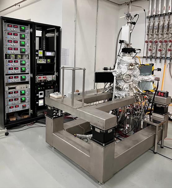
Low-temperature STM-MBE system (4 K STM under construction)
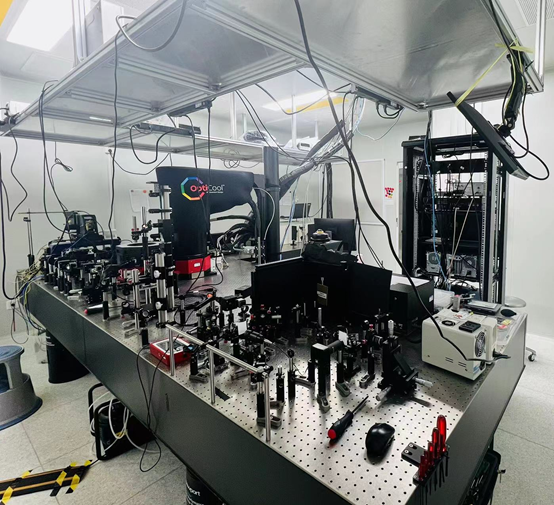
Optical characterization system (Quantum Design OptiCool, 2 K, 7 T)
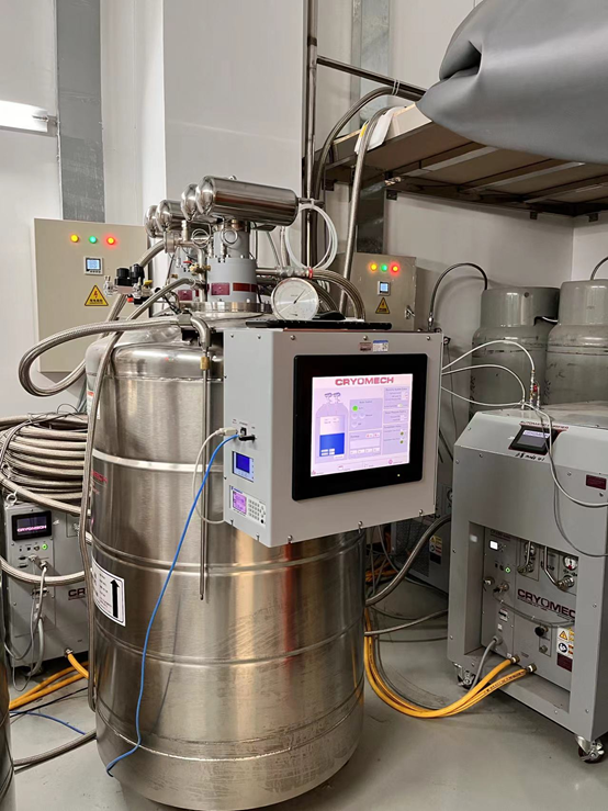
Liquid helium recovery system (Cryomech, 55 L/day)
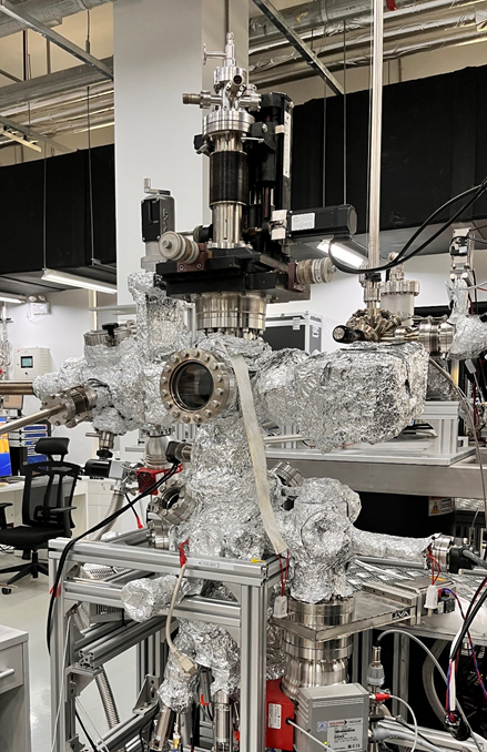
Miniaturized MBE system
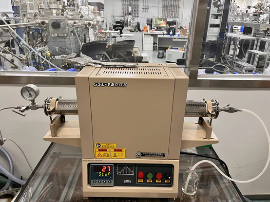
Tube furnace
Representative Publications from Team Members: (* corresponding authorship)
1. K. Chang*, J. W. D. Villanova, J.-R. Ji, S. Das, F. Küster, S. Barraza-Lopez*, P. Sessi*, S. S. P. Parkin*, Vortex-Oriented Ferroelectric Domains in SnTe/PbTe Monolayer Lateral Heterostructures. Adv. Mater. 2102267 (2021). doi:10.1002/adma.202102267
2. S. Barraza-Lopez*, B. M. Fregoso, J. W. Villanova, S. S. P. Parkin, K. Chang*, Colloquium: Physical properties of group-IV monochalcogenide monolayers. Rev. Mod. Phys. 93, 011001 (2021).
3. A. Bedoya-Pinto*, J.-R. Ji, A. Pandeya, P. Gargiani, M. Valvidares, P. Sessi, F. Radu, K. Chang*, and S. S. P. Parkin*. Intrinsic 2D-XY ferromagnetism in a van der Waals monolayer. arXiv:2006.07605.
4. K. Chang*, F. Küster, B. J. Miller, J.-R. Ji, J.-L. Zhang, P. Sessi, S. Barraza-Lopez, and S. S. P. Parkin*. Microscopic manipulation of ferroelectric domain walls in SnSe monolayers at room temperature. Nano Lett. (2020). doi:10.1021/acs.nanolett.0c02357
5. K. Chang* and S. S. P. Parkin*. Experimental formation of monolayer group-IV monochalcogenides. J. Appl. Phys. 127, 220902 (2020). (Invited Review) doi:10.1063/5.0012300
6. S.-Y. Yang, K. Chang*, and S. S. P. Parkin*. Large planar Hall effect in bismuth thin films. Phys. Rev. Research 2, 022029(R) (2020). doi:10.1103/PhysRevResearch.2.022029
7. K. Chang, B. J. Miller, H. Yang, H. Lin, S. S. P. Parkin, S. Barraza-Lopez, Q.-K. Xue, X. Chen, and S.-H. Ji. Standing waves induced by valley-mismatched domains in ferroelectric SnTe monolayers. Phys. Rev. Lett. 122, 206402 (2019). doi:10.1103/PhysRevLett.122.206402
8. K. Chang and S. S. P. Parkin. The growth and phase distribution of ultrathin SnTe on graphene. APL Materials 7, 041102 (2019). doi:10.1063/1.5091546
9. K. Chang, T. P. Kaloni, H. Lin, A. Bedoya-Pinto, A. K. Pandeya, I. Kostanovskiy, K. Zhao, Y. Zhong, X. Hu, Q.-K. Xue, X. Chen, S.-H. Ji, S. Barraza-Lopez, and S. S. P. Parkin. Enhanced Spontaneous Polarization in Ultrathin SnTe Films with Layered Antipolar Structure. Adv. Mater. 31, 1804428 (2019). doi:10.1002/adma.201804428
10. K. Chang, J. Liu, H. Lin, N. Wang, K. Zhao, A. Zhang, F. Jin, Y. Zhong, X. Hu, W. Duan, Q. Zhang, L. Fu, Q.-K. Xue, X. Chen, and S.-H. Ji. Discovery of robust in-plane ferroelectricity in the atomic-thick SnTe. Science 353, 274 (2016). doi:10.1126/science.aad8609
11. K. Chang, P. Deng, T. Zhang, H.-C. Lin, K. Zhao, S.-H. Ji, L.-L. Wang, K. He, X.-C. Ma, X. Chen, and Q.-K. Xue. Molecular beam epitaxy growth of superconducting LiFeAs film on SrTiO3(001) substrate. EPL 109, 28003 (2015). doi:10.1209/0295-5075/109/28003
12. J. Liu, K. Chang, S.-H. Ji, X. Chen, and L. Fu. Apparatus and methods for memory using in-plane polarization. US patent, No.: US 9,959,920 B2. Date of patent: May 1, 2018.
 中文
中文 Email
Email QCloud
 Log in
