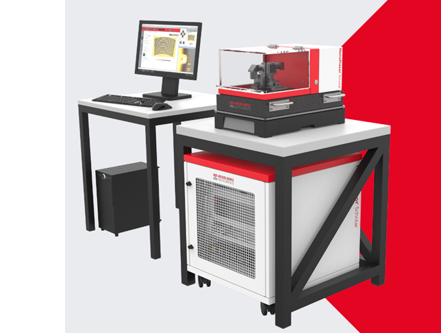
3D NANOFRAZOR (SCHOLAR)
2020/9/18 11:52:54

Overview:NanoFrazor lithography is the fastest and most versatile of all Scanning Probe Lithography techniques. Core of the NanoFrazor technology is an ultra-sharp heatable probe tip which is used for writing and simultaneous inspection of complex nanostructures. The heated tip creates arbitrary, high-resolution nanostructures by local sublimation of resists. Standard pattern transfer methods like lift-off or etching can be applied. It is installed in the glovebox to enable nanolithography of sensitive materials in inert conditions.
Applications:rapid prototyping of 3D quantum devices.
Features:
Resolution below 20 nm
In-situ high-speed AFM topography imaging
Samples size up to 50 x 50 mm2
Closed-Loop Lithography
Precise markerless overlay and stitching using in-situ AFM
No damage of sensitive materials (no electron or ion beams)
Alternative patterning mode: direct nanoscale thermal conversion
Small footprint
Easy to use (no wet development, no vacuum, etc.)
 中文
中文 Email
Email QCloud
 Log in
