Progress in the study of semiconductor quantum dot array
2024/11/11
Recently, Hongqi Xu's group from BAQIS/Peking University, in collaboration with Jianhua Zhao-Dong Pan's group from the Institute of Semiconductors of the Chinese Academy of Sciences, has achieved an integrated device carrying two single-electron charge sensors and a coupled one-dimensional quintuple-quantum-dot (QQD) array based on a semiconductor indium arsenide (InAs) nanowire, utilizing the cutting-edge nanofabrication techniques. The high tunability of electron charge states and the electronic coupling strength between quantum dots in the coupled quintuple-quantum-dot array is revealed through ultra-precision cryo-electronic measurements. This provides a physical platform for the construction of advanced quantum processors based on semiconductor nanowire materials. This work, entitled "One-dimensional quantum dot array integrated with charge sensors in an InAs nanowire", was published in Nano Letters, on October 28, 2024.

FIG. 1 (a) SEM image of the inear quintuple-quantum-dot array integrated with charge sensors; (b) Schematic diagram of device structure and measurement circuits.
Semiconducting nanowires with strong spin-orbit interactions is highly used in pursuing advanced quantum processors and novel state of matters, such as spin qubits, Andreev spin qubits and Majorana-based topological qubits. Therein, quantum dots made of these nanowires are particularly important since quantum dots are either a key element for constructing quantum states or used as a sensitive tool for quantum state readout. Coupled quantum dots in a linear array are manifested as a highly tunable platform to run analog quantum simulations, such as Fermi-Hubbard model and Su-Schrieffer-Heeger (SSH) model. Thus, semiconductor nanowires are considered one of the best material systems to build coupled quantum dots and study their charge/spin properties. However, the number of quantum dots in semiconductor nanowires is still limited to a few. It is mainly due to the challenge of process technology integrating charge sensors on such one-dimensional systems aside from their length limitation. In order to advance the quantum hardware built on semiconductor nanowires, expanding the number of coupled quantum dots together with charge sensors becomes the focus of current research.
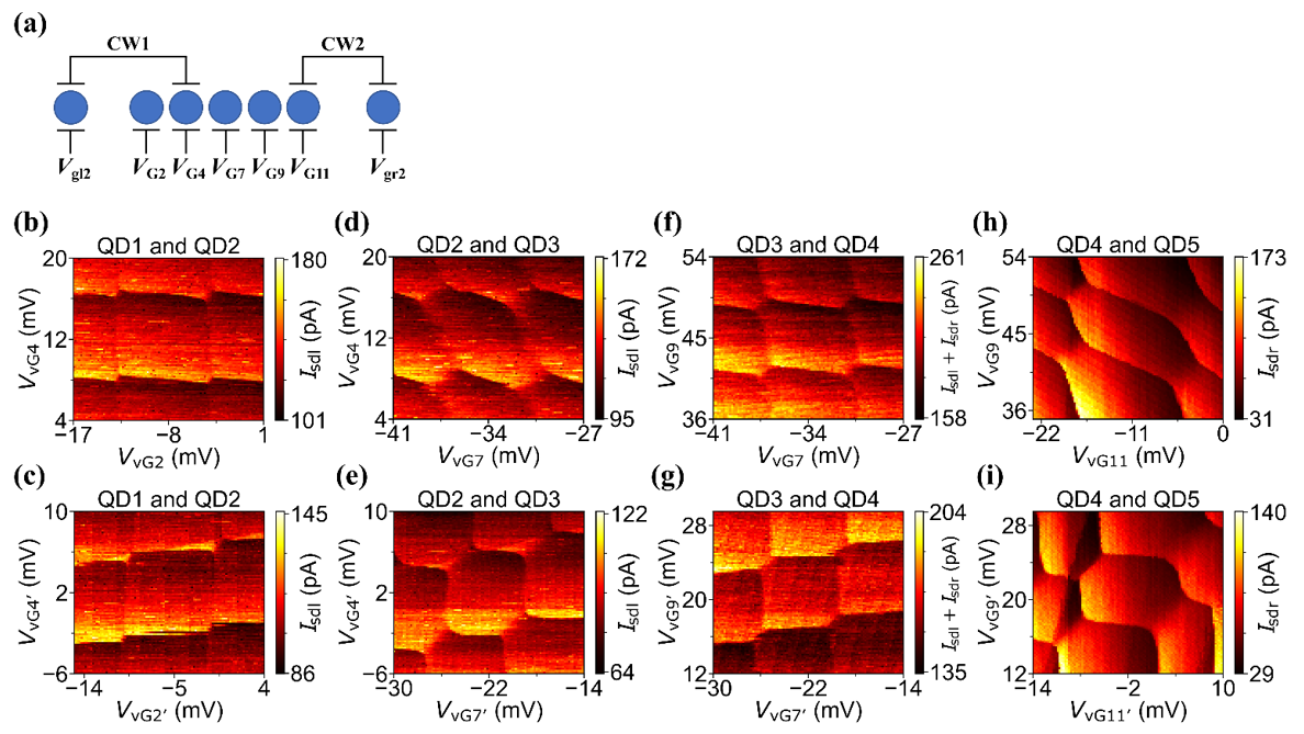
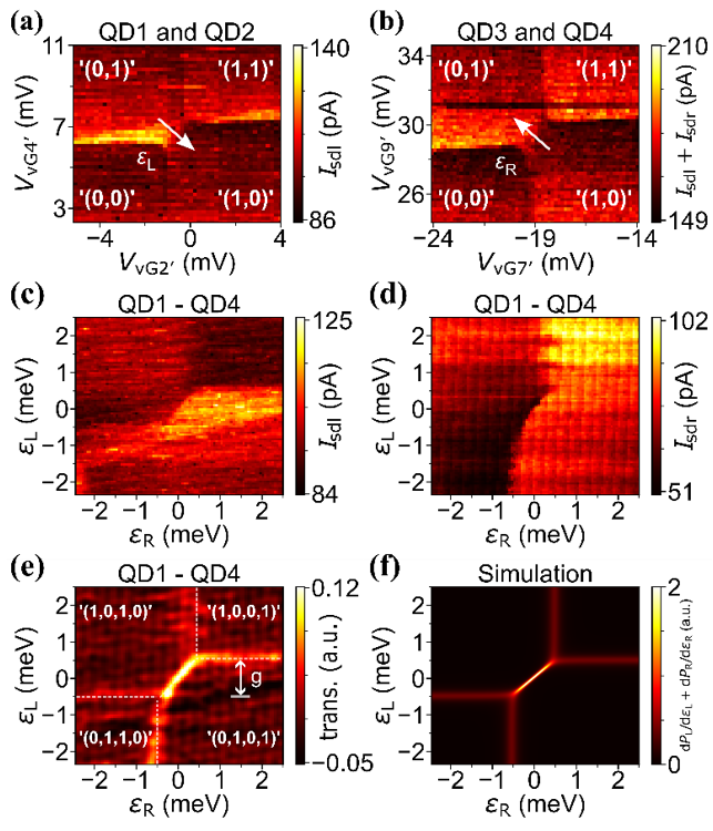
Researchers have developed a one-dimensional coupled quintuple-quantum-dot device based on a single semiconductor InAs nanowire grown by molecular beam epitaxy (MBE) utilizing ultra-fine local gate technology. The charge sensors are integrated on both sides to readout the charge state configurations (as shown in Fig. 1). By using the "virtual gate" technique, linearly recombining the control voltages of each gate, the crosstalk effects between the gates are effectively eliminated achieving independent tuning of the energy levels of each quantum dot in the quintuple-quantum-dot array (as shown in Fig. 2). After that, four dots in the array are used to form two double-quantum-dots (DQDs). The capacitive coupling strength between the two DQDs can be controlled to be as large as ~240 GHz, which is several times of that in GaAs- and Si-based quantum dot arrays. The ultra-strong coupling strength is likely due to the pretty thin diameter of the InAs nanowire (~30 nm) and the well isolation of the nanowire from surrounding environment. Especially, the latter leads to relatively weak capacitive coupling between quantum dots in semiconductor nanowires and their environment, thereby enhancing the coupling strength between neighboring dots. A theoretical simulation based on a 4-dimensional Hamiltonian exhibits well agreement with the experimental data (as shown in Fig. 3), supporting the above analysis.

FIG. 2 Electron charge stability diagrams of a coupled linear quintuple-quantum-dot array obtained by "virtual gate" technique.

FIG. 3 Extraction of capacitive coupling strength between two DQDs in semiconductor InAs nanowire quantum dot array and the numerical simulation results.
Yi Luo, a doctoral candidate from Peking University and an intern from BAQIS, is the first author of the above research results. Pan Dong, research fellow from Institute of Semiconductors, Chinese Academy of Sciences, Ji-Yin Wang, associate research fellow from BAQIS, and Hongqi Xu, professor of Peking University and chief scientist of BAQIS, are corresponding authors. Collaborators also include Xiao-Fei Liu, Zhi-Hai Liu and Shili Yan, assistant research fellows from BAQIS, Han Gao, postdoctoral fellow from BAQIS, Weijie Li and Haitian Su, PhD students from Peking University, and Jianhua Zhao, research fellow from Institute of Semiconductors, Chinese Academy of Sciences. This work was supported by grants from the National Natural Science Foundation of China and other projects.
Paper link:
https://pubs.acs.org/doi/10.1021/acs.nanolett.4c03646
 中文
中文 Email
Email QCloud
 Log in
