Dr. Kai Chang and colleagues report the oscillation of electronic-band-gap size in an ultrathin semiconductor in Physical Review Letters
2023/07/11
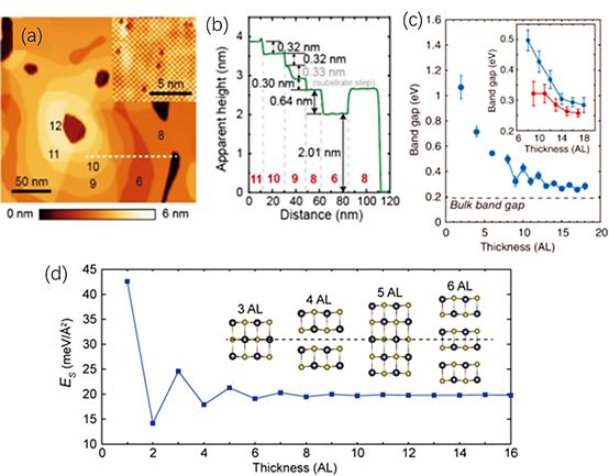
Recently, scientists from Beijing Academy of Quantum Information Science (Dr. Kai Chang, Dr. Haicheng Lin), Tsinghua University (Prof. Qi-Kun Xue, Prof. Xi Chen, Prof. Shuai-Hua Ji), and Hong Kong University of Science and Technology (Dr. Mengli Hu, Prof. Junwei Liu) published in Physical Review Letters on July 5th, 2023 to report that when the thickness of a two-dimensional semiconducting PbTe film is reduced from 18 to 2 atomic layers, the size of its electronic band gap exhibits an even-odd layer oscillation. This phenomenon is induced by the alternation in crystalline symmetry between even- and odd-layer thick films. This discovery provides new insights for the electronic structure engineering of atomic-scale semiconductor in next-generation nanoelectronics.
Band gap of semiconductors fundamentally governs their electronic and optical properties for practical applications. Therefore, tuning the size of band gap has always been a central topic in the engineering of semiconductors. The industry often relies on the change of material composition to tune the band gap size, while the crystalline size effect is often viewed as a detrimental effect. However, in this work, the authors demonstrate that in ultrathin semiconducting films, even one atomic layer’s change in thick can alter the crystalline symmetry, and thus effectively tune the band gap size.
PbTe, a material that has been broadly used in infrared optoelectronics and high-speed electronic devices, and potentially useful in topological quantum computing, is the main character of this study. The authors have precisely determined the thickness of each terrace in a PbTe film (ranging from 2 to 18 atomic layers), and demonstrated that an even-layer thick terrace has a relatively larger band gap than that in the neighboring odd-layer thick terraces. This phenomenon is ascribed to the different crystalline symmetries (mirror symmetry for odd-layer, and glide symmetry for even-layer) of films with different thicknesses. This work shows that even without doping, people can still engineer the band gap size of an ultrathin semiconductor in a broad range, just by slightly changing the number of its atomic layers. Therefore, one material could evolve into a series of materials with different band gaps, hence greatly improve the freedom of semiconductor electronic structure engineering.

The band gap exhibits oscillations with thickness due to even-odd layer effects in PbTe thin films. (a) Film topography. (b) Height profile. (c) Experimental data of band gap evolution. (d) Theoretical calculation of the surface energy and the "dimerization" of atomic layers in even-layer thick films.
This work is funded by the National Key R&D Program of China, National Natural Science Foundation of China, Beijing Municipal Science & Technology Commission, as well as Hong Kong Research Grants Council.
Article Links: https://doi.org/10.1103/PhysRevLett.131.016202
 中文
中文 Email
Email QCloud
 Log in
