Defect-free Nanowelding Achieved in 2D Semiconductors
2024/07/09
Currently, there is no ideal solution for crystal alignment in the welding of two-dimensional semiconductors, posing one of the biggest challenges in nanofabrication technology. Recently, Dr. Kai Chang from Beijing Academy of Quantum Information Science (BAQIS), in collaboration with Max Planck Institute for Microstructure Physics in Germany and the University of Arkansas in the United States, has achieved strict directional movement and lattice alignment of two-dimensional semiconductor SnSe nanosheets using the anisotropic frictional forces on the graphene surface through scanning tunneling microscope probe manipulation and in-situ annealing methods. This demonstrates the defect-free welding of SnSe nanosheets. The related work was published in the journal “Advanced Materials” on June 20, 2024, under the title “Defect-Free Nanowelding of Bilayer SnSe Nanoplates.”
As electronic devices continue to shrink, the demands on nanoscale manufacturing precision have risen sharply. Laboratory techniques are broadly categorized into "top-down" and "bottom-up" approaches. The "top-down" method, such as electron beam lithography (EBL), achieves 10-nanometer precision. However, it struggles to meet higher precision requirements for manufacturing and can damage materials during the etching process. In contrast, the "bottom-up" approach, including the technique known as "nanowelding," has emerged over the past decades. It utilizes mechanical micromanipulation for assembling nanoscale elements such as quantum dots, nanowires, and nanosheets. Subsequently, these components are fused together via methods like heating, laser irradiation, or application of pressure. Nanowelding technique enables the fabrication of diverse structures as required, similar to piecing together building blocks. Early nanowelding techniques focus on metallic materials, such as noble metal nanowires. The weak directional nature of metal bonds makes it easier to achieve interface relaxation under various annealing methods, resulting in interfaces with fewer defects. However, the strong directional nature of ionic or covalent bonds in semiconductor materials can lead to numerous defects at the interface if there is a rotation angle between the crystals on either side, severely affecting the mechanical and electrical properties of the welded structure. Therefore, crystal alignment in welding has become a significant challenge, especially for the welding between two-dimensional semiconductors, for which there is currently no particularly ideal solution.
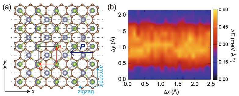
SnSe is a two-dimensional semiconductor with orthogonal lattice symmetry. Its rectangular cell's lattice constant along one direction closely matches that of graphene, enabling a lattice coupling. Along this direction, the SnSe lattice appears integrated within the zigzag chains formed by carbon atoms in graphene, significantly enhancing the frictional force and preventing relative slippage. In contrast, the absence of lattice coupling in the other direction results in minimal frictional force, allowing SnSe nanosheets to slide freely, guided by the carbon zigzag chains. Therefore, the research team proposed using the graphene lattice to guide the orientation and movement of SnSe nanosheets, ensuring precise crystal alignment. When two SnSe nanosheets are assembled together using a scanning tunneling microscope probe, in-situ annealing can completely eliminate the gaps between them, achieving a nanowelding process that is atomically defect-free.

Figure 1 The alignment of the SnSe nanosheets with graphene along the armchair orientation leads to a pronounced anisotropy in the frictional forces that SnSe encounters, particularly when traversing the a1 and a2 crystallographic axes.

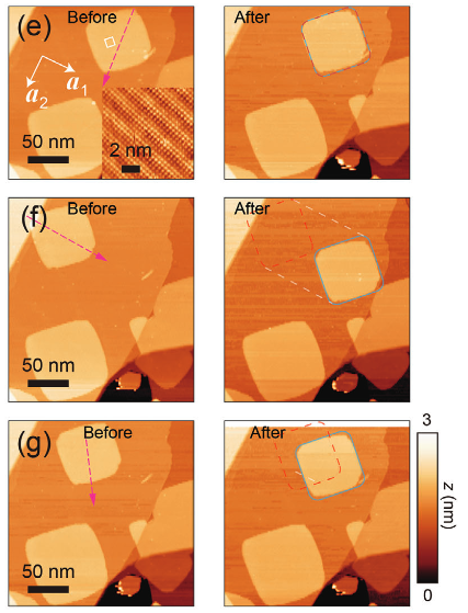
Figure 2 Upon applying the STM tip to exert force on the SnSe nanosheet across various orientations, it was observed that the nanosheet only shifted along the a1 direction.

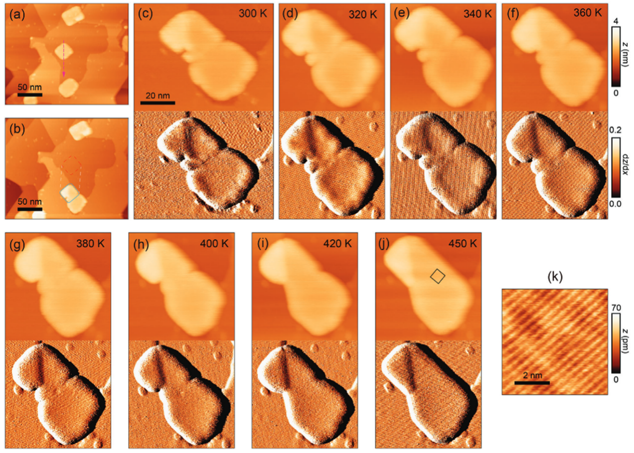
Figure 3 Defect-free nanowelding achieved through precise alignment and in-situ annealing of SnSe nanosheets.
Anisotropic frictional forces at the interfaces of various two-dimensional material heterostructures are a well-documented phenomenon. The previously mentioned method can be readily adapted for nanowelding a wider array of two-dimensional materials and is also applicable to the manipulation of one-dimensional and zero-dimensional materials. The exceptional precision of scanning tunneling microscope probes, down to the sub-atomic level, suggests that the nanowelding technique could enable device feature sizes surpassing current nanofabrication capabilities. This advancement holds substantial promise for the development of microelectronic devices and solid-state qubits at the atomic scale.
The first author of this study is Jingrong Ji at Max Planck Institute for Microstructure Physics. The corresponding authors are Dr. Kai Chang from BAQIS, Prof. Stuart S. P. Parkin from Max Planck Institute for Microstructure Physics, and Prof. Salvador Barraza-Lopez from the University of Arkansas.
Link:https://onlinelibrary.wiley.com/doi/full/10.1002/adma.202312199
 中文
中文 Email
Email QCloud
 Log in
