Advances achieved in nanowire-based Majorana systems by topological quantum computation group of BAQIS
2022/04/18
The topological quantum computation group from Beijing Academy of Quantum Information Sciences (BAQIS), in collaboration with researchers from Tsinghua University, Institute of Semiconductors of Chinese Academy of Sciences, etc., has recently achieved several progresses in exploring a new Majorana nanowire material and developing new method of distinguishing Majorana zero modes (MZMs) from Andreev bound states. These achievements have been published in four papers on international physical journals including Physical Review Letters, Physical Review B and Physical Review Materials.

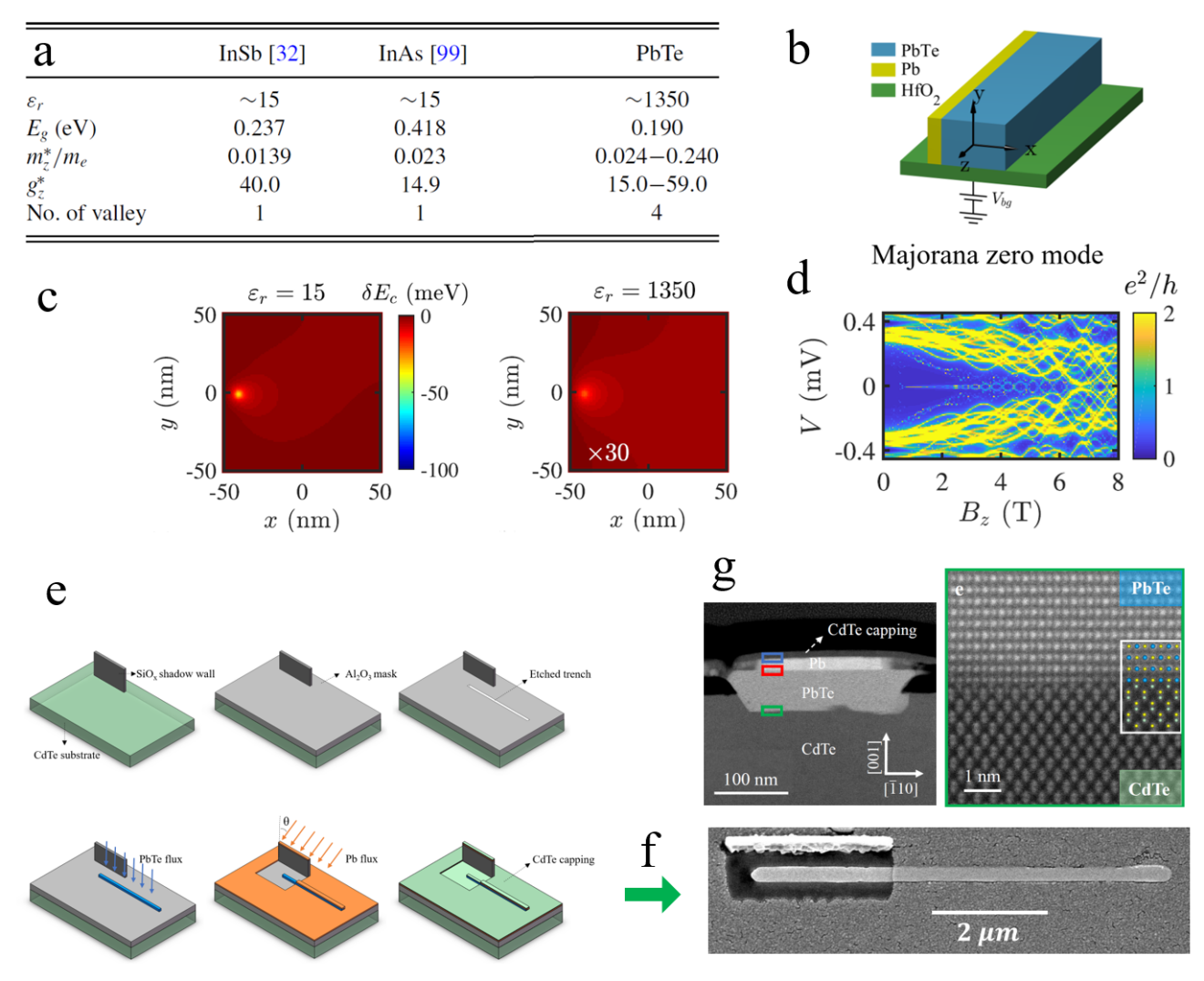
Fig.1: (a) Table of parameters for different materials, including InAs, InSb and PbTe. (b) The schematics of the PbTe-Pb device. (c) Impurity-induced potential distribution of the cross section of the nanowire, for InAs/InSb (the left panel) and PbTe (the right panel), respectively. (d) Majorana zero mode induced conductance spectrum from numerical simulation. (e) The schematics of PbTe-Pb nanowire device with the chosen direction. (f) The electron microscope figure of one PbTe-Pb sample. (g) The TEM figure of the sample cross section and the PbTe-CdTe interface.
Majorana zero modes in hybrid superconductor-semiconductor nanowires hold promise towards topological quantum computation. So far, the nanowires are mostly InAs- and InSb-based and the superconductor is dominantly Al. Though significant progress has been achieved over the last decade, these two III-V-based material platforms now face great challenges due to the existence of disorder in currently the best devices. To solve this problem, the topological quantum computation group of BAQIS instead investigated an IV-VI semiconductor, i.e., PbTe, as an alternative host of Majorana zero modes. Briefly, PbTe is a narrowband semiconductor with both a large spin-orbit coupling and a large Landé g factor. It also has a huge dielectric constant that is normally two orders larger in amplitude than that of InAs and InSb (Fig. 1a). Importantly, this huge dielectric constant leads to a stronger and more efficient screening on disorder-induced electrostatic potential. As the consequence, PbTe devices are expected to have a higher tolerance of disorder and impurity influences. Indeed, following the numerical analysis of the device configuration in Fig.1b, the degree of disorder of a PbTe device is less than one thirtieth of that of InAs and InSb ones (Fig.1c). In addition, theoretical analysis is also carried out to investigate the advantages to choose Pb (instead of Al) as the superconductor material of the heterostructure. Briefly, in comparison to Al, Pb has a much larger (almost ten times) superconducting gap and a stronger critical magnetic field, which provides a better topological protection on Majorana zero modes. With new choices of both semiconductor and superconducting materials, the characteristics of the PbTe-Pb hybrid nanowire have been theoretically investigated, with the predicted requirement for entering topological superconducting phase (Fig. 1d). This work entitled “Numerical study of PbTe-Pb hybrid nanowires for engineering Majorana zero modes” has recently be published on Physical Review B, with its first author Zhan Cao (an assistant researcher of BAQIS), and corresponding authors Dong E. Liu, Ke He, and Hao Zhang (three joint researchers of BAQIS)1.
Accompanied with theory, the experimental researchers of topological quantum computation group has develop the technique of direct growing PbTe-Pb hybrid nanowire devices with molecular beam epitaxy after a continuous exploration/effort of more than two years. Combining selective area growth (SAG) and shadow wall growth, they have achieved PbTe-Pb hybrid nanowires and complex structures on pre-pattered CdTe substrate in a molecular beam epitaxy chamber (Fig. 1e-g). More importantly, compared to the SAG InAs and InSb nanowires, the advantage of PbTe nanowire is its lattice matching with the CdTe substrate, which minimizes an important source of disorder. The study provides a complete toolbox of fabricating high-quality scalable topological quantum computation devices. This experimental work, entitled “Selective area epitaxy of PbTe-Pb hybrid nanowires on a lattice-matched substrate”, is published in Physical Review Materials2. The first authors are Yuying Jiang, Shuai Yang, Lin Li, Wenyu Song and Wentao Miao. Prof. Hao Zhang and Prof. Ke He are the corresponding authors.

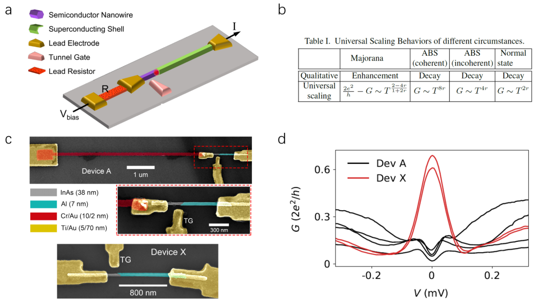
Fig.2: (a) The theoretical schematics of a dissipative device. (b) Four universal behaviors of the temperature dependence of the conductance. (c) The STM photos of devices with (the upper one) and without (the lower one) dissipation. (d) The conductance peak through a dissipation-free (the red curve) zero-energy Andreev bound state splits into two smaller peaks near zero bias, under the influence of a strong dissipation.
In hybrid nanowire devices, the detection of Majorana zero modes through one-probe transport measurement is currently under hot debated in the scientific community, as zero-bias conductance peaks can be induced by both Majorana zero modes and Andreev bound states. Recently, members of topological quantum computation of BAQIS have developed a new method to experimentally tell Majorana zero modes from Andreev bound states. Theoretically, with the introduction of a resistance (Fig.2a), particles through the system couple to plasmonic excitations, inducing the effective many-body phenomenon “environmental Coulomb blockade” that counter-influences the particle transport in devices. It has been predicted [see Physical Review Letters 111, 207003 (2013)] by Dong E. Liu (a joint researcher of BAQIS) that a proper choice of dissipation leads to the splitting of zero-bias conductance peaks induced by Andreev bound states, while those induced by Majorana zero modes remain. As the latest progress, the Dong E. Liu group proposes specific universal features (Fig.2b) to tell Majorana zero modes from Andreev bound states. Indeed, after introducing interaction between electrons and the environmental bosons, Majorana transport signals become remarkably different in comparison to that from topologically trivial Andreev bound states. This work has been published on Physical Review Letters, with the title “Universal conductance scaling of Andreev reflections using a dissipative probe"3.
Inspired by the theory, the experimental group in Tsinghua University has managed to couple a resistor (with multiple kilo-Ohm resistance) to an InAs-Al semiconductor junction. When the Al lead is in the metallic state, the observed transport signal through the junction, especially its power-law feature, agrees remarkably with the environmental Coulomb blockade theory. When the Al lead is superconducting, the Andreev bound state can be tuned to zero energy by controlling the magnetic field and the gate voltages. In this regime, the experimental group manages to observed the zero-bias peak splitting due to the resistance-induced environmental Coulomb blockade (Fig.2d). This work has been published on Physical Review Letters, with the title "Suppressing Andreev bound state zero bias peaks using a strongly dissipative lead"4.
"Now the most formidable challenge of the nanowire approach of topological quantum computing is how to fabricate complex structures of hybrid nanowires and at the same time significantly reduce the disorder level of the devices.” Ke He says, "The new candidate Majorana system we discovered—SAG PbTe-Pb hybrid nanowires epitaxied on CdTe substrates—has a big advantage in overcoming the problem. Maybe it could beat III-V materials in achieving topological quantum computing.”
Works above are supported by the National Science Foundation of China, the Ministry of Science and Technology of China, Beijing Municipal Science and Technology Commission, Tsinghua University Independent Research Program, State Key Laboratory of Low-Dimensional Quantum Physics of Tsinghua University, and Frontier Science Center for Quantum Information.
Reference:
1. Zhan Cao, Dong E. Liu, Wan-Xiu He, Xin Liu, Ke He, and Hao Zhang(2022), Numerical study of PbTe-Pb hybrid nanowires for engineering Majorana zero modes. Phys. Rev. B 105, 085424
2. Yuying Jiang, et al. (2022) Selective area epitaxy of PbTe-Pb hybrid nanowires on a lattice-matched substrate. Phys. Rev. Materials 6, 034205
3. Donghao Liu, Gu Zhang, Zhan Cao, Hao Zhang, and Dong E. Liu (2022), Universal Conductance Scaling of Andreev Reflections Using a Dissipative Probe. Phys. Rev. Lett. 128, 076802
4. Shan Zhang, et al. (2022), Suppressing Andreev Bound State Zero Bias Peaks Using a Strongly Dissipative Lead. Phys. Rev. Lett. 128, 076803
 中文
中文 Email
Email QCloud
 Log in
